


- Free 15-day Returns
$22.49
Ships from China.

Meet Your Seller

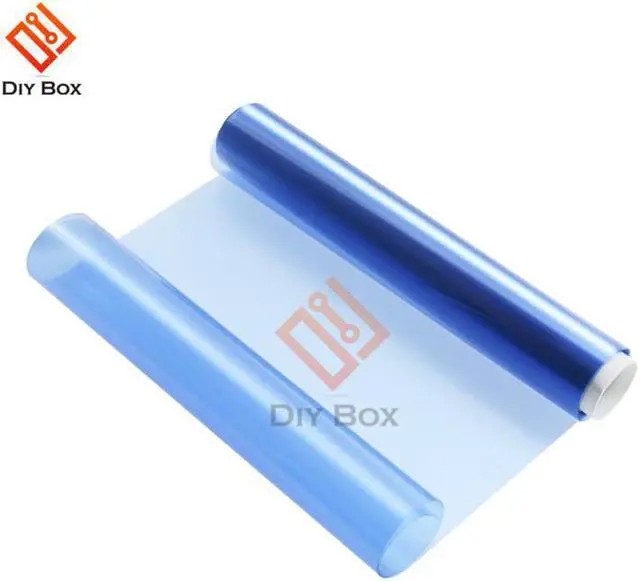
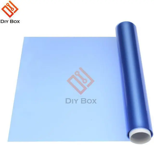
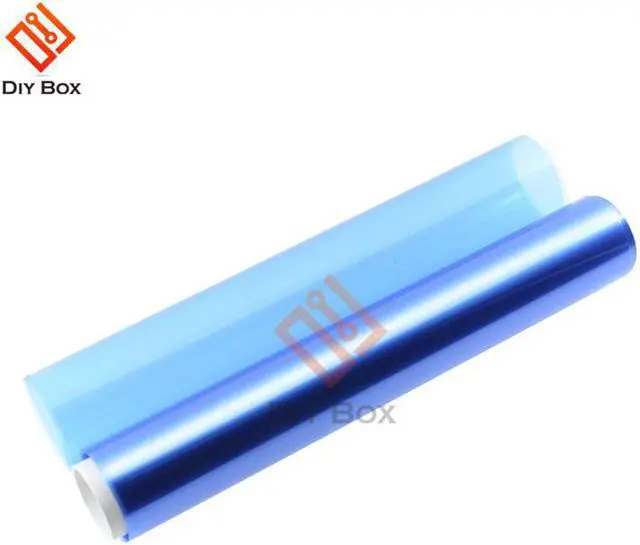
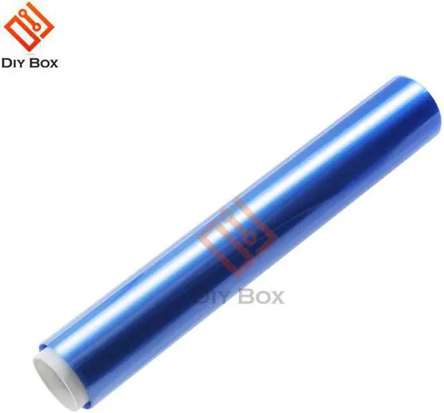
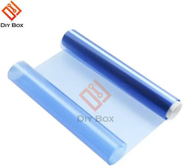
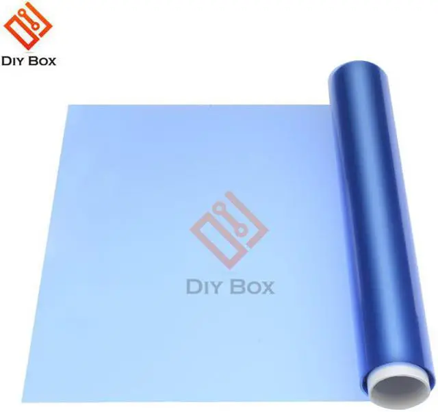
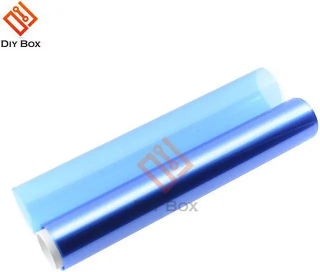


2M PCB Portable Photosensitive Dry Film For Circuit Photoresist Sheets For Plating Hole Covering Etching 15cmx200cm
- 2M PCB Portable Photosensitive Dry Film For Circuit Photoresist Sheets For Plating Hole Covering Etching 15cmx200cm
+
+
Overview
Specs
Reviews
Origin:CN(Origin)
Gift Package:No
2M PCB Portable Photosensitive Dry Film For Circuit Photoresist Sheets For Plating Hole Covering Etching 15cmx200cm
Features
- Photographic film, also known as dry film, is used to make PCB board, stick it on top of the PCB, it will become a sensitive circuit board.
- Suitable for plating, hole coveringand the etching process.
- Excellent ability to cover holes
- High Resolution
- Excellent adhesion to almost all surfaces
- Image clarity after exposure
- Front-panel is very clean after developed
Size: 15 x 200 cm / 5.91'' x 78.74''
Color: As pictures shown
How to use it :
1. Clean your board. Cut dry film a little larger than your board.
2. Apply Resist: This Photoresist has 3 layers, the top and bottom layers are clear protective layer, so at the first, you need remove one protective layer, the easy way is to use two small pieces of scotch tape. Then apply the middle layer on board.
3. Expose: Place your negative artwork over the rest protective layer.
4. Develop: Remember: you need NEGATIVE film developer, Remove the rest protective layer on the film. After 3 minutes take board out of developer and hold under running water to check,you can always place it back in the developer if needs more time.
Etching
The dry film is resistant to most of the acid etching solution, the PH value can be resistant to most alkaline etching solution between PH8.0 ~8.5.
Cover hole
1.5 mil dry film can fully cover a 0.25 inches thickness hole.
Plating
The dry film is available in most common use of the plating bath, no wrinkles, no color.
Package include
1 roll photosensitive dry film
Gift Package:No
2M PCB Portable Photosensitive Dry Film For Circuit Photoresist Sheets For Plating Hole Covering Etching 15cmx200cm
Features
- Photographic film, also known as dry film, is used to make PCB board, stick it on top of the PCB, it will become a sensitive circuit board.
- Suitable for plating, hole coveringand the etching process.
- Excellent ability to cover holes
- High Resolution
- Excellent adhesion to almost all surfaces
- Image clarity after exposure
- Front-panel is very clean after developed
Size: 15 x 200 cm / 5.91'' x 78.74''
Color: As pictures shown
How to use it :
1. Clean your board. Cut dry film a little larger than your board.
2. Apply Resist: This Photoresist has 3 layers, the top and bottom layers are clear protective layer, so at the first, you need remove one protective layer, the easy way is to use two small pieces of scotch tape. Then apply the middle layer on board.
3. Expose: Place your negative artwork over the rest protective layer.
4. Develop: Remember: you need NEGATIVE film developer, Remove the rest protective layer on the film. After 3 minutes take board out of developer and hold under running water to check,you can always place it back in the developer if needs more time.
Etching
The dry film is resistant to most of the acid etching solution, the PH value can be resistant to most alkaline etching solution between PH8.0 ~8.5.
Cover hole
1.5 mil dry film can fully cover a 0.25 inches thickness hole.
Plating
The dry film is available in most common use of the plating bath, no wrinkles, no color.
Package include
1 roll photosensitive dry film
Warranty & Returns
Warranty, Returns, And Additional Information
Warranty
- Please contact the Seller directly for warranty information. Warranty information may also be found on the Manufacturer's website.
- CONTACT
Return Policies
- Return for refund within: 15 days
- Return for replacement within: 30 days
- This item is covered by Shengkedianzi Return Policy
Manufacturer Contact Info
- For a directory of all our manufacturers, please click below.
- Manufacturers Directory
LOADING...